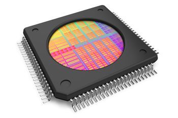
 Semiconductor materials are the foundation of modern electronics - radios, computers, telephones, and many other electronic devices such as transistors, solar cells, diodes, rectifiers and integrated circuits. Silicon is used to create most semiconductors commercially although many other materials are used, including germanium, gallium arsenide, and silicon carbide.
Laser marking systems can sort and inspect semiconductor wafers for fast, efficient and error-free marking of both sides of 300mm wafers.
TLM Laser engineers are respected worldwide and among the best in the business within the semiconductor industry. With a wealth of experience accumulated over a number of years on laser marking systems and can offer service, maintenance call outs and spare parts.
TLM are the exclusive distributors in the UK and Ireland for Innolas GmbH wafer marking products.
For more information see InnoLas Wafer Marking & Sorting Systems