Wafer Marking and Wafer Sorting
In the semiconductor industry, traceability is a necessary evil. To meet statutory regulations, electronic devices must be marked. However, this is a non-value added process. That’s why manufacturers choose the speed, lack of consumables and silicon handling compatibility that laser marking delivers.
Hard Mark or Soft Mark?
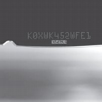 There are two types of mark associated with silicon surfaces. The first is an etched mark or “hard mark”. In this instance, the laser is used to ablate the silicon and leave an etch typically 12 to 25mm microns deep. The second is a “soft mark”. This is a shallow annealed mark where the laser wavelength is adjusted so that the beam’s energy does not ablate the surface but rearranges the molecules on the part’s surface.
Tight Tolerances
Silicon like other materials used in semiconductor manufacturing such as germanium and gallium is a very sensitive surface for marking. Minor changes in laser power applied to the material’s surface can cause differences in mark appearance and consistency. In addition, applying laser energy so close to the active components can result in device damage. That’s why specifications for hard and soft marking depths have very tight tolerances - tolerances that depend critically on the precision and quality of the laser marking system itself.
Marking and Sorting Leaders
With a reputation for superior precision and performance gained from the implementation and set-up of almost 1000 systems, InnoLas Semiconductor GmbH is a European market leader in the development and manufacture of laser sysems for wafer marking, sorting and inspection. The company specialises in meeting the individual needs of each customer, tailoring solutions that use different optical set-ups to achieve the optimum process quality on all semiconductor materials. The company carries DIN EN ISO 9001 quality management accreditation through TÜV Austria.
The range of InnoLas wafer marking systems can handle 100mm up to 450mm wafers and caters for both low and high volume users. Innolas wafer sorting systems can all automatically sort, split and merge wafers. The sorting range starts with a stand-alone six cassette system right up to a fully automatic 7 loadport system.
If you would like to know more about the InnoLas range of wafer marking and sorting systems, please contact sales@tlm-laser.com