TLM Laser is the distribution partner for InnoLas’ market leading Semiconductor products.
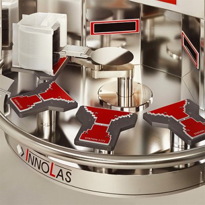
InnoLas Semiconductor GmbH is a European market leader in the development and manufacturing of laser systems for wafer marking sorting and inspection. Thanks to many years of technological cooperation with its customers in wafer marking and sorting processes along with the practical experience gained from the setup and implementation of almost a 1000 systems, InnoLas is aware of the specific technological requirements of the semiconductor industry and offers a wide range of proven products that can be optimized for a variety of customer applications.
In order to ensure superior performance in the productivity and efficiency of wafer processing required by the Semiconductor Industry, InnoLas guarantees maximum availability and fail-safe operation of its systems. This offer is complemented by TLM’s reliable and swift field service and thorough end user training programs.

InnoLas Data Sheets